FESEM
Field Emission Scanning Electron Microscope
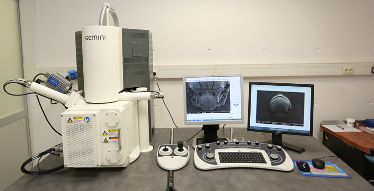
By focusing electrons accelerated at high voltage onto the sample, the sample surface is scanned, enabling interaction between the incident electrons and the sample's atoms. The image is obtained by collecting these interactions via appropriate detectors, passing them through signal amplifiers, and transmitting them to the cathode ray tube display. These images provide detailed information regarding the particle size and particle arrangement of the sample.
Electron Gun: Schottky Field-Emission Magnification Range: 12x – 1,000,000x Acceleration Voltage: 0.02 – 30 Kv Vacuum System: * High Vacuum Mode (HV) (≤10⁻⁶ mbar) Variable Pressure Mode (VP) (0.01 – 1.33 mbar)
SE2 Detector (Everhart-Thornley type) and In-Lens Detector: Used in HV mode to collect secondary electrons (SE) to obtain high-resolution topographical images of the sample surface.
VPSE Detector: Used in VP mode for the analysis and imaging of non-conductive, uncoated samples such as polymers and glass.
AsB Detector: Used in HV mode to collect backscattered electrons (BSE) to obtain two-dimensional images based on atomic contrast and crystallographic orientation.
EDS Detector: Used to determine the atomic concentrations of the sample. Its mapping feature provides information about the distribution of elements within the sample.
STEM Detector: Used to obtain microstructure images of biological tissues/samples at up to 30 kV.
Copyright © 2019 PAU - ILTAM